
Ultrasonic Spray Coating of Photoresist for Panel Level Packaging
Panel-level packaging has emerged as a core advanced packaging technology in the semiconductor industry, featuring high integration, high production efficiency and low unit cost, and is widely applied in high-end chip manufacturing. Unlike traditional single-package packaging processes, panel-level packaging production needs to complete photoresist coating operations on ultra-large-area substrates, which integrate hundreds to thousands of independent packaging units. The overall flatness, thickness consistency and surface uniformity of the photoresist coating on the entire panel directly determine the precision of subsequent lithography, etching and packaging processes, putting forward extremely high requirements on coating accuracy and process stability.
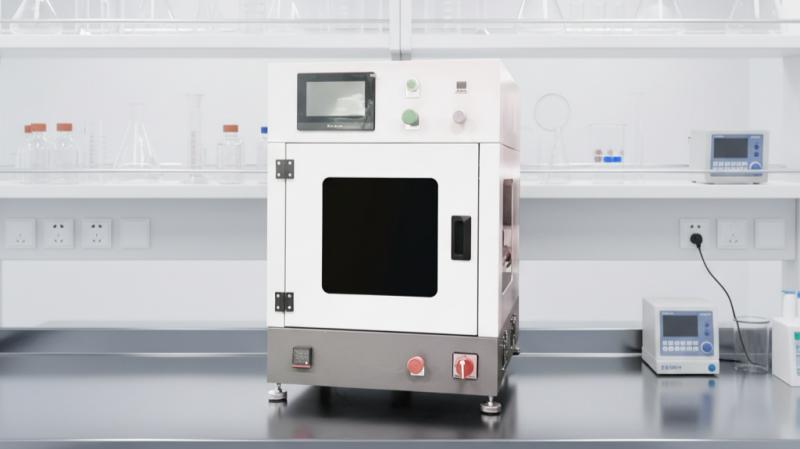
Professional photoresist coating processes for panel-level packaging are designed to adapt to the complex structural characteristics of advanced packaging substrates. The optimized coating technology can form smooth and uniform photoresist films on various key substrate surfaces including redistribution layers, bonding pads, dielectric layers and micro-patterned features. It effectively fits the fine structural dimensions of advanced packaging, provides a stable and high-quality material foundation for precision lithography procedures, and ensures the alignment accuracy and structural integrity of each independent packaging unit on the large panel, greatly improving the yield of mass packaging production.
The ultrasonic spray coating process, as an efficient and reliable photoresist coating method for panel-level packaging, solves many technical pain points of traditional coating processes. This process can achieve full-coverage and consistent-thickness photoresist coating on the entire large-size packaging panel, thoroughly improving common defects in conventional coating technologies such as liquid pooling, surface streaks, edge thickness deviation and local coating missing. These defects are extremely likely to cause lithography offset, pattern distortion and packaging failure in subsequent production, and the optimized spray coating process can effectively avoid such production risks.
In particular for large rectangular packaging panels commonly used in mass semiconductor production, the traditional spin coating process has obvious technical limitations. Spin coating relies on centrifugal force to spread photoresist, which will generate severe material splashing and loss, resulting in extremely high raw material waste. Meanwhile, affected by centrifugal force gradient and panel edge effects, spin coating is prone to form uneven film thickness distribution, with obvious thickness differences between the panel center and edges. In contrast, the ultrasonic spray coating process adopts non-contact atomization coating, which not only greatly reduces photoresist material consumption and production cost, but also realizes ultra-uniform film formation on large-area panels, stably meeting the high-precision and high-consistency production standards of modern panel-level advanced packaging.
About Cheersonic
Cheersonic is the leading developer and manufacturer of ultrasonic coating systems for applying precise, thin film coatings to protect, strengthen or smooth surfaces on parts and components for the microelectronics/electronics, alternative energy, medical and industrial markets, including specialized glass applications in construction and automotive.
Our coating solutions are environmentally-friendly, efficient and highly reliable, and enable dramatic reductions in overspray, savings in raw material, water and energy usage and provide improved process repeatability, transfer efficiency, high uniformity and reduced emissions.
Chinese Website: Cheersonic Provides Professional Coating Solutions
