Ultrasonic Soldering Iron Soldering PCB Gold Fingers
Ultrasonic Soldering Iron Soldering PCB Gold Fingers – Sonic4Lab
In electronic product interconnect systems, gold fingers are specialized connectors. These are gold-plated pads located along the edge of a PCB, named for their finger-like shape. As connectors between the PCB and the motherboard, gold fingers not only ensure reliable signal transmission but also protect the edges of the circuit board from damage.
The production process for gold fingers primarily involves two gold plating methods. Chemical nickel gold is relatively inexpensive and easy to solder, but it is soft and thin (typically 2-5μm), making it unsuitable for frequent plugging and unplugging. Electroplated hard gold offers greater hardness, thickness, and wear resistance, making it suitable for areas like gold fingers and PCB contacts that require constant plugging and unplugging. Its thickness can be adjusted according to requirements, though a thicker thickness increases the cost.
The electroplating hard gold process involves rigorous steps: first, 3-6μm of nickel is plated on copper, followed by 1-2μm of hard gold (often reinforced with cobalt to increase surface resistance) on the nickel. Finally, surface treatment and quality inspection are performed. In addition, the edges of gold fingers must be chamfered at specified angles (20°, 30°, 45°, 60°, or 90°, with 30°-45° being the most common) to facilitate connector insertion. Some gold fingers are designed with varying lengths to facilitate insertion and removal. Segmented gold fingers are recommended for durable electronic products.
The electroplating process has numerous limitations: The inner layers at the PCB edge must be free of copper to prevent copper exposure during beveling. Plated holes, SMDs, and pads must maintain a minimum distance of 1.0mm from the gold fingers (except for some VIPs that are filled and leveled through electroplating). The length of plated pads must not exceed 40mm. The distance between the gold fingers and the edge must be 0.5mm. Furthermore, gold fingers must avoid contact with solder mask or silkscreen, as this may affect communication or insertion and removal.
Gold is used for gold fingers due to its excellent conductivity and corrosion resistance. Alloys mixed with nickel or cobalt offer even greater wear resistance. IPC standards clearly define gold finger designs: the gold plating must contain 5%-10% cobalt to enhance rigidity; the electroplating thickness must be no less than 2 microinches and no more than 50 microinches, with common specifications including 0.031-inch and 0.062-inch. Prototypes often use thinner plating to save costs; and gold finger designs must be visually inspected with a magnifying glass to ensure a smooth surface and no excess plating, as well as tested with a tape test to ensure adhesion.
In terms of design, the process and design of gold finger designs can affect performance such as impedance, loss, and crosstalk. In high-speed PCB design, impedance adjustment is often achieved by hollowing out the metal layer under the pad or using a reference interlayer. Optimization can also be verified through simulation or test boards. Standard products such as PCIe and memory modules have clear gold finger design specifications, and proper design can effectively improve signal integrity.
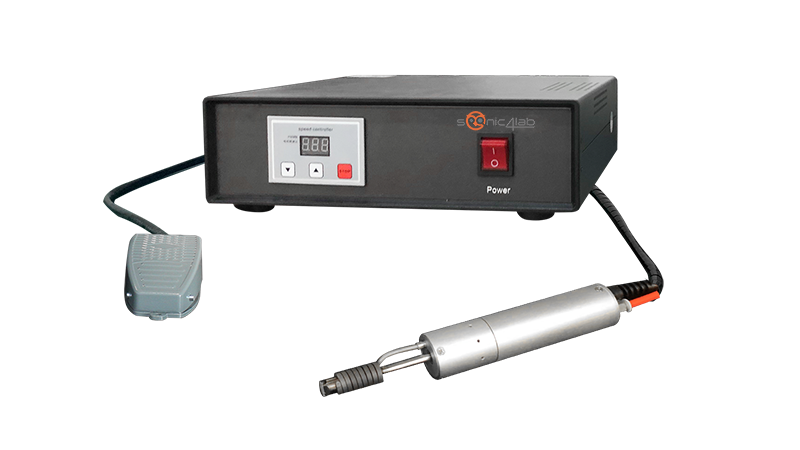
The design and process control of gold finger designs are crucial to the performance of electronic products, especially high-speed products, where every detail must be carefully considered to ensure reliability. Ultrasonic soldering irons, with their core advantage of flux-free soldering, demonstrate irreplaceable value in precisely connecting thin gold ribbons to gold-plated pads on PCBs. When working with thin gold ribbons as thin as 250μm and tiny gold-plated pads measuring approximately 2mm, they eliminate the need for flux to remove the oxide layer. Instead, they utilize high-frequency mechanical vibrations of 20kHz-40kHz to induce plastic deformation at the soldering interface. This, combined with localized high temperatures, breaks down and peels off the oxide layer on the metal surface, directly achieving atomic bonding between the gold ribbon and the gold-plated pad.
If you want to purchase equipment, please click here