Ultrasonic Soldering Cracking Multi-layer FPC Soldering
In the wave of electronic products moving towards lightweight and high integration, flexible printed circuit boards have become core components in fields such as mobile phones, wearable devices, and automotive electronics due to their strong flexibility, lightweight volume, and high space utilization. In order to meet the increasingly complex functional requirements of devices, single-layer flexible printed circuits are gradually being replaced by multi-layer flexible printed circuits – by stacking multiple layers of circuits, higher signal transmission efficiency and component integration can be achieved. However, this also brings key challenges to the soldering process: control of alignment accuracy and avoidance of thermal damage in multi-layer flexible printed circuits.
The reason why the alignment welding of multi-layer flexible printed circuits has become a process bottleneck lies in two major pain points. Firstly, strict precision requirements are required. The size of each solder pad in multi-layer flexible printed circuits is often in the micrometer range, and the interlayer solder pads need to be completely aligned to ensure the continuity of the circuit. If the alignment deviation exceeds 0.1mm, it is highly likely to cause faults such as short circuits and poor contacts, directly affecting the reliability of the product; Secondly, the substrate has high thermal sensitivity. Flexible printed circuit substrates are mostly made of polymer materials such as polyimide, which have limited high-temperature resistance. Traditional processes such as hot air welding and iron soldering rely on high-temperature heating to melt the solder, which often leads to substrate deformation, circuit oxidation, and even damage to interlayer bonding structures, reducing product life.
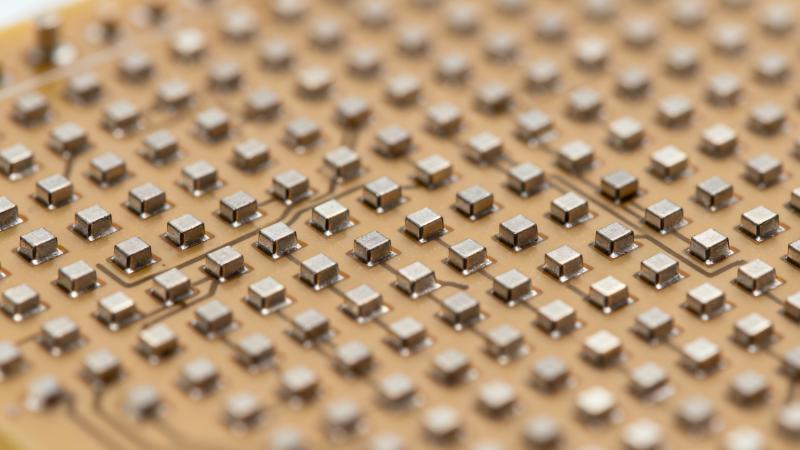
Ultrasonic soldering technology breaks through these limitations from a theoretical perspective. The core logic is to use high-frequency ultrasonic vibrations of 20-40kHz to convert mechanical energy into local thermal energy, causing plastic flow of solder at lower temperatures. At the same time, relying on precision visual positioning systems and mechanical transmission structures, accurate alignment of multi-layer flexible printed circuits is achieved. In the specific process flow, the first step is the pre-treatment of the solder surface, which removes the oxide layer and impurities on the surface of the flexible printed circuit solder pad through micro etching or plasma cleaning to ensure solder wettability; The second step is intelligent alignment, where the visual system captures the coordinates of the solder pads of each layer of flexible printed circuit in real time, guiding the robotic arm to accurately stack multiple layers of boards. The alignment error can be controlled within 0.05mm; The third step is ultrasonic welding, where the soldering head applies stable vibration energy and pressure to quickly fill the gap between the solder pads, forming a high density solder joint without voids.
This technological advantage is particularly prominent in practical scenarios. In the flexible screen module of smartphones, multi-layer flexible printed circuits need to be connected to the display driver chip and the motherboard. The low heat input of ultrasonic soldering can avoid residual images or damage to the flexible screen due to high temperature, while precise alignment ensures the stability of signal transmission; In the field of wearable devices, the soldering space for multi-layer flexible printed circuits is limited, and ultrasonic soldering can achieve reliable connection of micro solder joints without the need for complex fixtures; In automotive electronics, multi-layer flexible printed circuits need to withstand high and low temperature cycles and vibrations. The solder joints formed by ultrasonic soldering have high mechanical strength and strong fatigue resistance, which can effectively reduce the risk of failure during long-term use. In addition, ultrasonic soldering also has the characteristic of strong automation adaptability, which can seamlessly connect with the production line and greatly improve the efficiency of mass production.
With the continuous improvement of electronic device integration, the number of layers in multi-layer flexible printed circuits will continue to increase, and the line spacing will be further reduced, which puts higher demands on soldering technology. In the future, ultrasonic soldering technology will be upgraded towards higher frequency vibration control and AI visual positioning optimization, further improving alignment accuracy and process stability. It can be said that ultrasonic soldering is not only the core technology support for current multi-layer flexible printed circuit alignment soldering, but also will help the flexible electronics industry continue to break through towards thinner, more reliable, and higher integration.
About Sonic4Lab
Sonic4Lab was founded to ultrasonic instruments including ultrasonic soldering iron, ultrasonic impact treatment, ultrasonic knife and so on. Our customers are Research and Development laboratories and companies for production applications. We use state-of-the-art equipment and in-depth experience to develop accessible solutions for emerging applications.