The Truth About Gold-Plated PCBs: Easy Soldering
Among PCB surface treatments, immersion gold is highly sought after for its long-lasting properties, smooth pads, and excellent solderability. However, its high cost deters many. Many believe its solderability is due to the gold coating, and even believe that the thicker the gold layer, the better the soldering. This is a misunderstanding.
The truth is, the excellent solderability of gold-plated boards isn’t due to the gold, but rather to the nickel layer beneath it. During soldering, the extremely thin gold layer quickly dissolves into the solder, allowing the solder to directly contact and wet the nickel layer, forming a stable intermetallic compound (such as Ni₃Sn₄), ensuring the mechanical strength and electrical connection reliability of the solder joint. The gold layer is virtually absent from the solder interface.
The true function of the gold layer is both a protector and a sacrifice. It seals out air and moisture, preventing oxidation of the nickel layer. Once the nickel oxidizes, forming nickel oxide, it severely hinders solder wetting. The gold layer also ensures pad flatness, making it suitable for soldering fine-pitch components and extending storage life.
It’s important to note that immersion gold cannot be applied directly onto copper. Otherwise, at high temperatures, the copper will diffuse into the gold, forming a brittle compound that can affect solder joint quality. The nickel layer effectively prevents this diffusion.
With this understanding, you know there’s no need to blindly pursue immersion gold. For the same number of circuit boards, immersion gold treatment costs thousands of yuan more than tin-spraying, and even more than OSP. Considering your actual needs, there’s no need to blindly choose immersion gold; it can ensure quality while effectively reducing costs.
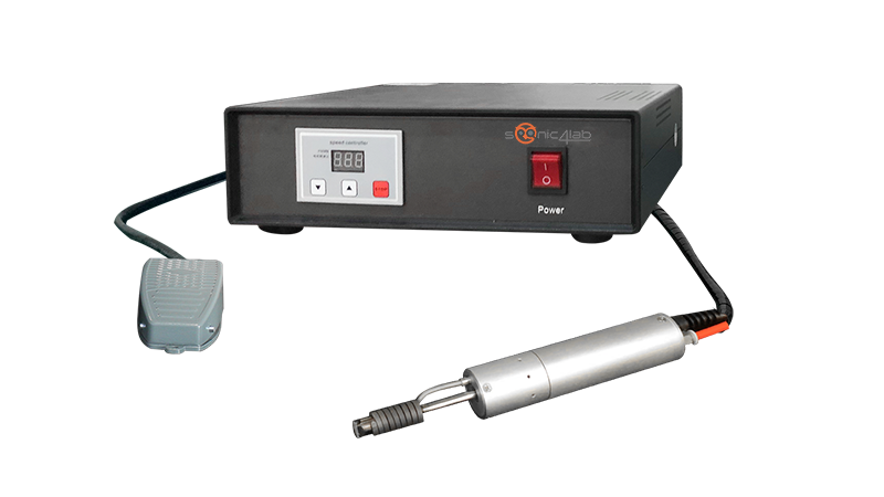
Ultrasonic soldering irons, with their core advantage of flux-free soldering, demonstrate irreplaceable value in precisely connecting thin gold ribbons to gold-plated PCB pads. When faced with a thin gold ribbon only 250μm wide and a tiny gold-plated pad about 2mm in size, it does not rely on flux to remove the oxide layer. Instead, it uses high-frequency mechanical vibrations of 20kHz-40kHz to allow the welding contact surface to undergo plastic deformation under the action of energy, while generating local high temperatures, causing the oxide layer on the metal surface to be broken and peeled off, directly achieving atomic bonding between the gold ribbon and the gold-plated pad.
If you want to purchase equipment, please click here