Project Description
Fabrication Of Microfluidic Chip
Fabrication Of Microfluidic Chip – Spray Microfluidic Chip Coating
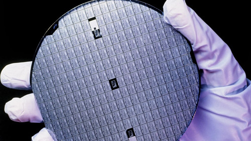
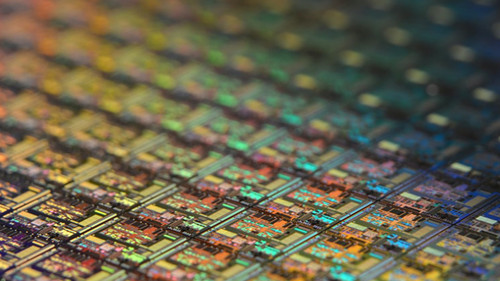
What is a microfluidic chip
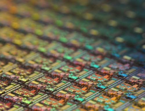
Microfluidic Chip (MicrofluidicChip), also known as Lab-on-a-Chip or biochip. It uses MEMS technology to microfilm a large laboratory system on a glass or plastic substrate, thereby replicating the entire process of complex biological and chemical reactions and completing experiments quickly and automatically. It is characterized by constructing fluid-containing channels, reaction chambers and other functional components on a micrometer scale, and manipulating the movement of micrometer-sized fluids in tiny spaces, thereby constructing a complete chemical or biological laboratory.
This technology will bring disruptive breakthroughs in diagnostic fields such as genes, immunity, microbes, and clinical chemistry, making it possible to diagnose and prevent early diagnosis and prevention of many diseases that threaten human health, such as cancer and cardiovascular and cerebrovascular diseases. The combination of biochips and bio-targeted drugs has promoted clinical medicine towards personalized medical diagnosis and treatment.
With the gradual development of microfluidic chip technology and the demand for microanalysis technology, chip configuration designs have become more abundant, and a series of chip configurations with different forms and multiple microchannel network structures have emerged. For example, the network shapes of the separation channels of the electrophoresis chip mainly include: linear, spiral, curved serpentine, polygonal, folded, etc. Due to the complexity and diversity requirements of biochemical analysis, the development of microfluidic chip technology tends to be combined and integrated. It is often necessary to integrate multiple functional units on a chip substrate, such as chemical reactors, bioreactors, and filter devices. Wait for the analysis and testing of various samples for DNA sequencing and mutation point detection, amino acid, protein, cell detection and drug screening. Based on the need for high-throughput and fast separation, parallel operation of multi-channel arrays is the development trend of microfluidic chips. The number of channels on the chip has grown from 12 channels and 96 channels to 384 channels.
Preparation of microfluidic chip
Microfluidic chips integrate various units with different functions through microfabrication technology, such as microreaction cells, micropumps, microvalves, detection units, etc. The micro-channel processing technology is different from the integrated circuit chip which is mainly based on the two-dimensional and shallow depth processing of silicon materials. Two important indicators of microchannels in microfluidic chips are the aspect ratio and the interface shape of the microchannel.
The aspect ratio refers to the ratio of the depth feature to the width feature of the microstructure formed on the substrate, and it is difficult to process the high aspect ratio structure. For the direct processing method, the shape characteristics are related to the direction of corrosion, that is, isotropy or anisotropy will form different geometric features; for the replication processing methods, such as hot molding and molding, the microchannel geometry is directly It is related to template shape and processing technology.
Manufacturing technology of microfluidic chip
(1) Lithography and etching technology
Traditional lithography and etching techniques used to make semiconductor and integrated circuit chips are the most basic of microfluidic chip processing technology. It uses photoresist, mask and ultraviolet light for microfabrication. The technology is mature and has been widely used to make microstructures on silicon, glass and quartz substrates. Lithography and etching technology consists of three processes: film deposition, photolithography and etching. Complex microstructures can be completed by repeating the three steps of film deposition-photolithography-etching multiple times.
Before photolithography, a film must be covered on the surface of a clean substrate. The thickness of the film is from several angstroms to tens of microns. This process is called film deposition. The film can be divided into the epitaxial layer of the device working area according to the different performance, the masking film that limits the area expansion, the insulating dielectric film that plays the role of protection, passivation and insulation, and the conductive metal film used as the electrode lead and the device interconnection. Film materials commonly include silicon dioxide, silicon nitride, borophosphosilicate glass, polysilicon, conductive metals, photoresist, refractory metals, etc. The main methods of manufacturing and processing thin films are oxidation, chemical vapor deposition, evaporation, sputtering, and ultrasonic spray deposition.
The surface of the film is evenly covered with a layer of photoresist, and the process of transferring the microfluidic chip design pattern on the mask to the photoresist layer through the principle of exposure imaging is called photolithography. Lithography technology generally consists of the following basic processes:
① Pretreatment of the substrate.
The surface of the substrate is purified by degreasing, polishing, pickling, and water washing to ensure good adhesion of the photoresist to the surface of the substrate.
②Gluing.
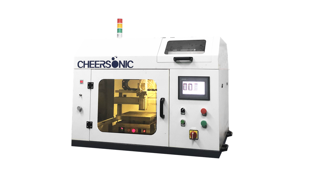
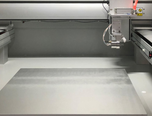
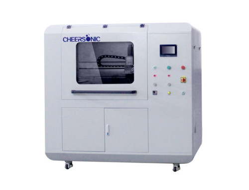
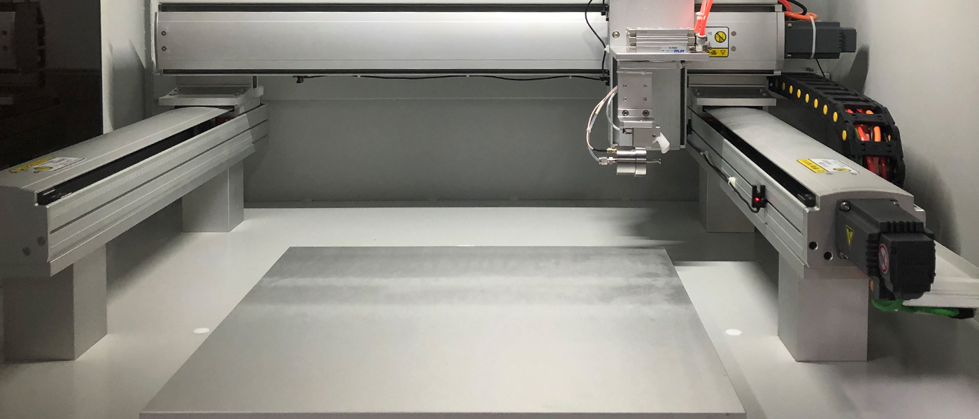
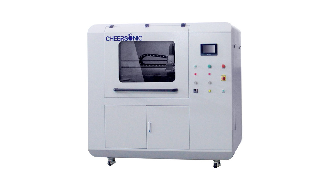
A layer of photoresist with good viscosity and appropriate thickness is uniformly coated on the surface of the treated substrate. If the film is too thin, it is easy to generate pinholes, and the corrosion resistance is poor; if it is too thick, it is not easy to develop completely, and the resolution will be reduced. The actual thickness of the photoresist is related to its viscosity and is inversely proportional to the square root of the spinning speed of the spinner. Glue coating methods include spin coating, brush coating, dipping, spray coating, etc. Among them, ultrasonic spraying method is newly applied in this industry, and ultrasonic spraying technology is used for photoresist coating. Compared with traditional spin coating and dip coating processes, it has the advantages of high uniformity, good microstructure encapsulation, and controllable coating area. In the past ten years, it has been fully demonstrated that the 3D microstructure surface photoresist coating using ultrasonic spraying technology is significantly higher than the traditional spinner in terms of microstructure wrapping and uniformity. Painted. The ultrasonic spraying system of Cheersonic can precisely control the flow rate, coating speed and deposition amount. Low-speed spray forming defines atomized spray as a precise and controllable mode to avoid overspray when producing a very thin and uniform coating. The ultrasonic spraying system can control the thickness from sub-micron to more than 100 microns, and can coat any shape or size.
③Bake before.
At a certain temperature, the solvent in the photoresist solution is volatilized to enhance the adhesion of the photoresist to the substrate and the wear resistance of the film. The temperature and time of the pre-bake are determined by the type and thickness of the photoresist, and an electric thermostat, hot air or infrared heat source is often used.
The pre-baking temperature and time should be appropriate. If the temperature is too high or the time is too long, it will leave a base film during development or decrease the sensitivity of the sensitivity, and small islands will appear during corrosion; if the temperature is too low or the time is too short, it will cause pinholes after development. Increase, or produce floating glue, figure distortion, etc.
④ Exposure.
Cover the substrate with a photolithography mask with the required chip pattern prepared, and selectively irradiate the photoresist with ultraviolet rays through the mask. The photoresist irradiated by light undergoes a chemical reaction. In actual operation, the exposure time is determined by the photolithography film, the thickness of the adhesive film, the intensity of the light source, and the distance between the light source and the substrate. The exposure methods include chemical exposure, contact and proximity copy exposure, and optical projection imaging exposure.
⑤Development.
Use photoresist matching developer to remove exposed photoresist (positive photoresist) or unexposed photoresist (negative photoresist) through chemical methods. The choice of developer and development time has a great influence on the development effect. The principle of selecting developer is that the part of the film that needs to be removed has high solubility and fast dissolution rate, and the part that needs to be retained has low solubility. The development time depends on the type of photoresist, the thickness of the film, the type of developer, the development temperature and the method of operation.
⑥ Hard film.
Clean the developed substrate and bake it at a certain temperature to completely remove the solvent or moisture remaining in the adhesive film after development, so that the adhesive film and the substrate adhere closely to prevent the adhesive layer from falling off and strengthen the adhesive film Its own corrosion resistance. The temperature and time of film building should be appropriate.
Etching is the process of transferring the planar two-dimensional pattern on the photoresist layer to the film and then processing it into a certain depth microstructure on the substrate.
According to different etchant states, the etching process can be divided into two categories: wet etching and dry etching. Wet etching is an etching method in which the etched substance is stripped off by a chemical reaction between a chemical etching solution and the etched substance. Most wet etching is isotropic corrosion that is not easy to control.
It is characterized by high selection ratio, good uniformity, and less damage to silicon wafers. It is suitable for almost all metal, glass, plastic and other materials. The disadvantage is that the fidelity of the pattern is not strong, and lateral undercutting often occurs at the same time as the lateral corrosion, so that the minimum line width of the etched pattern is limited.
Dry etching refers to a process in which high-energy beams react with the surface film to form volatile substances, or directly bombard the film surface to be corroded. Its biggest feature is that it can realize anisotropic etching, that is, the etching rate in the vertical direction is much higher than that in the horizontal direction, so as to ensure the fidelity after the transfer of fine patterns. The basis of dry etching is plasma.
When processing microfluidic chips by photolithography, a photolithography mask must be manufactured first. The basic function of the mask is that when the substrate is irradiated by the light beam, it produces different light absorption and transmission capabilities in the pattern area and the non-pattern area. The computer graphics system is used to convert the mask pattern into a data file, and then the exposure light source, iris diaphragm, worktable and lens in the pattern generator are controlled through a dedicated interface circuit, and the required pattern is carved on the mask material. Or use a computer to convert the structure diagram of the design microchannel into an image file through CAD software, and then print the image on a transparent film with a high-resolution printer. This transparent film can be used as a mask for photolithography, and can basically meet the mask requirements of microfluidic chips.
(2) Hot pressing method
Hot embossing (hot embossing) is a widely used chip manufacturing technology that quickly replicates electrophoretic microchannels, and is suitable for thermoplastic polymer materials such as PMMA and PC. The hot pressing mold can be a metal wire with a diameter of less than 50 μm or a micro-channel bone sheet positive film with etched protrusions, such as nickel-based positive molds, single crystal silicon positive molds, glass positive molds, and micromachined ones. Metal male model. This method can be copied in large quantities, the equipment is simple, and the operation is simple, but the materials used are limited.
(3) Molding method
The male mold (protruding part of the required channel) is first made by photolithography and etching, and the liquid polymer material is poured, and then the cured polymer material is peeled off from the male mold to obtain the prepared micro-channel chip. The chip method is called the molding method. The key to the molding method is the choice of mold and polymer materials. The ideal material should have low adhesion to each other and be easy to demold.
The positive film of the microchannel can be made of silicon material, glass, epoxy-based SU-8 negative light glue and PDMS. Standard etching techniques can be used for silicon or glass anode films. The PDMS mold can be made by directly casting on a master mold made of silicon material, glass and other materials.
The polymer material used for pouring should have low viscosity and low curing temperature. Under the action of gravity, the microchannels and grooves on the mold can be filled. There are two types of materials available: curing polymers and solvent volatile polymers.
Although the molding method is limited to polymer materials, this method is simple and easy to implement. The chip can be copied in large quantities and does not require expensive equipment. It is a method for making cheap analysis chips.
(4) Injection molding method
The process of injection molding is to etch a negative electrophoresis chip on the silicon wafer through photolithography and etching technology, and use this negative mold for 24h electroforming to obtain a 0.5 cm thick nickel alloy mold, and then add the nickel alloy mold Thick, carefully processed into a metal injection mold, which is installed on an injection molding machine to mass produce polymer microfluidic chip substrates.
In the injection molding process, the mold production is complex, the technical requirements are high, and the cycle is long, which are the key steps in the entire process. A good mold can produce 300,000 to 500,000 polymer chips, with good repeatability, short production cycle, low cost, and suitable for the production of molded chips.
(5) LIGA technology
LIGA is an acronym for Lithographie, Galvanoformung, and Abformung in German. LIGA technology is composed of three links: photolithography, electroforming and plastic casting.
Quasi-LIGA technology uses ultraviolet light source to replace synchrotron radiation X-ray deep lithography in LIGA technology, and then performs subsequent micro-electroforming and micro-replication processes. It does not require synchrotron radiation X-ray lithography and special X-ray mask, which is conducive to mass production of micromechanical devices. According to the different process routes of ultraviolet deep lithography, quasi-LIGA technology can be divided into three types: multilayer lithography—LIGA, silicon mold deep etching—LIGA and SU-8 deep lithography—LIGA.
(6) Laser ablation method
Laser ablation is a non-contact microfabrication technology. It can directly process complex microstructures on metals, plastics, ceramics and other materials based on computer CAD data, and has been applied to the processing of micromolds and microchannels. This method requires high technical equipment, simple steps, no ultra-clean environment, and high accuracy. However, due to the high energy of the ultraviolet laser, there is a certain danger, so it needs to be operated in a standard laser laboratory, using safety protection equipment and protective glasses.
(7) Soft lithography
Soft lithography (soft lithography) is a new method of micro-pattern transfer and micro-manufacturing relative to the dominant photolithography in the field of micro-manufacturing. It uses self-assembled monolayers, elastic stamps and polymer molding technologies as examples. Basic new microfabrication technology. It can manufacture complex three-dimensional structures and irregular curved surfaces; it can be applied to a variety of materials such as biopolymers, colloids, glass, ceramics, etc.; there is no precision limit caused by related scattering, and it can reach a small size of 30 nm ~ 1 μm; Therefore, soft lithography is a cheap, convenient, and suitable technology for laboratory use.
The core of soft lithography technology is the elastic stamp, which can be made by photolithography and molding methods. PDMS is the most commonly used elastic stamp in soft lithography. The key technologies of soft lithography mainly include micro-contact printing, re-molding, micro-transfer molding, capillary molding, solvent-assisted molding and so on.
Soft lithography technology still has some defects, such as 1% shrinkage deformation after curing of PDMS, and under the action of toluene and ethane, the aspect ratio will expand to a certain extent; the elasticity and thermal expansion of PDMS make it difficult Achieving high accuracy also restricts the use of soft lithography in multi-level micromachining; because the elastic mold is too soft to obtain a large aspect ratio, too large or too small aspect ratio will lead to microstructure Deformed or twisted.
Nowadays, microfluidic chips have become a comprehensive cross-discipline covering a series of applied research fields including separation analysis, chemical synthesis, medical diagnostics, cell biology, neurobiology, systems biology, structural biology, microbiology, etc.
