
Photoresist Deposition for Microelectronics
Photoresist Deposition onto Unconventional Substrates for Microelectronics Manufacturing
Spin coating technology faces major limitations when applied to oversized, curved and specially shaped substrates in microelectronic fabrication. As an alternative, ultrasonic spray coating technology is capable of forming highly uniform and conformable photoresist films on the full surface and microstructures of such unconventional substrates. It facilitates high-precision photolithographic processing for cutting-edge optical, electronic, semiconductor and biomedical device fabrication, effectively eliminating common coating defects including liquid accumulation, streak marks and excessive edge bead formation. This coating method enables accurate regulation of film thickness and stable interfacial adhesion, and allows flexible adjustment of photoresist solvent formulations to optimize surface wetting and drying characteristics according to production demands.
Large-Scale Optical Devices and Display Panels
Ultrasonic spray deposition achieves full-area coating with precise edge thickness control for flat display panels, large-aperture lenses, diffractive optical elements, anti-reflection components and other free-form optical parts. Even on curved and non-planar substrate surfaces, the photoresist film can maintain excellent thickness uniformity after soft baking. This process is perfectly suited for the fabrication of AR/VR optical components, diffractive microstructures and high-precision photolithographic patterned structures.
Microfluidic Chips and Biosensor Substrates
For the manufacturing of microfluidic systems, biosensors and lab-on-a-chip devices, spray-coated photoresist exhibits superior adhesion performance on glass, multiple polymer materials (PMMA, COC, PDMS) and composite heterogeneous substrates. The precise atomization of coating droplets generates smooth, solvent-tolerant thin films with high pattern replication accuracy. This approach reduces photoresist material consumption while ensuring stable and consistent thickness of dielectric and polymer functional layers.
Metallic and Conductive Substrate Coating
Photoresist can be directly deposited on various metallic substrates including gold, platinum, copper, aluminum and stainless steel, supporting the manufacturing of electrochemical biosensors, micro-electro-mechanical systems (MEMS) and microwave radio-frequency circuits. Ultrasonic spray coating delivers uniform film coverage on reflective metallic surfaces with poor wettability, and realizes fine-tuning of film thickness to ensure high-precision pattern forming on microstructures and sidewall surfaces.
Flexible Electronics and Roll-to-Roll Production
Aiming at the fabrication requirements of flexible electronic devices, organic thin-film transistors (OTFTs) and flexible solar cells, ultrasonic spray coating features low solvent consumption and low-temperature processing characteristics, which is fully compatible with continuous roll-to-roll mass production workflows. With high material transfer efficiency and closed-loop process regulation, this technology cuts down the usage of photoresist and chemical solvents while maintaining stable coating accuracy in large-scale production.
Specialized Polymer and Dielectric Layer Patterning
For the preparation of photonic crystals, polymer-based MEMS, metamaterials and optical waveguides, spray-deposited photoresist can form conformal masking layers and template structures on micro and nano-structured surfaces. The process boasts strong compatibility with various photoresist materials, including positive photoresist, negative photoresist and UV-curable photoresist systems.
Core Technical Advantages
– Achieves uniform and conformable photoresist coverage on oversized, curved and irregular substrates
– Significantly suppresses edge bead defects and improves overall photolithography resolution
– Supports closed-loop thickness regulation with excellent process repeatability and stability
– Features broad substrate compatibility, covering glass, diverse polymers, PDMS, metal materials and flexible thin films
– Boasts high material transfer efficiency, greatly reducing photoresist and solvent waste
– Adaptable to both batch-type intermittent production and continuous roll-to-roll large-scale manufacturing

EQUIPMENT SOLUTIONS
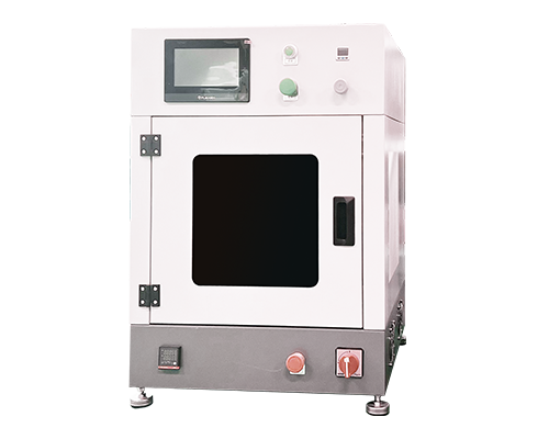
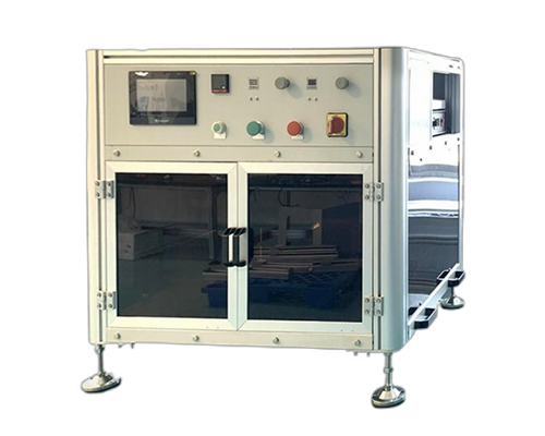
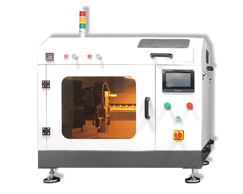
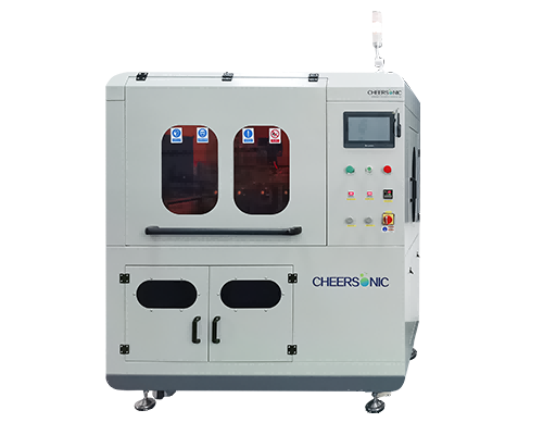
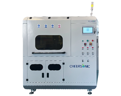
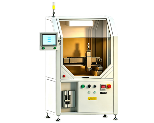
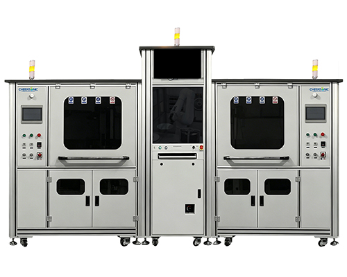
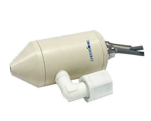
To reach our anytime via email please fill out the form below with your request and a company representative will reply to you. To find your local CHEERSONIC representative to connect directly click your region in the contact drop down menu.

Contact CHEERSONIC For immediate assistance please contact us the corporate headquarters during business hours at 6:00 am – 22:00 pm.
Tel: 0571-87910406
- Mobile: +86 13588732518
- Email: Market2@cheersonic.com
Add: 11-13 Chuangye Road, Changkou, Fuyang, Hangzhou, Zhejiang, China
