Photoresist Applications in IC Advanced Packaging
Background of Advanced Packaging Technology for Integrated Circuits
With the development of technologies such as 5G, artificial intelligence, and the Internet of Things, semiconductor devices are upgrading towards smaller size, faster speed, and higher energy efficiency. Advanced packaging of integrated circuits has become a core link in solving chip integration and performance challenges, and is also an important direction for continuing Moore’s Law.
Current mainstream advanced packaging technologies include: flip chip, bump technology, fan-in wafer-level packaging, fan-out wafer-level packaging, 2.5D packaging, through-silicon vias (TSVs) for CMOS image sensors, and fan-out panel-level packaging.
The packaging process requires organic, inorganic, and metal materials to create passivation layers, metal redistribution layers, conductive structures, and chip reconstruction. Photoresist is a key patterning material.
Classification and Market Overview of Photoresists
1. Classification by Exposure Light Source Wavelength
g-line (436nm), i-line (365nm), KrF (248nm), ArF (193nm), EUV (13.5nm).
2. Market Size
The domestic photoresist market size was approximately RMB 12.1 billion in 2023 and is projected to reach approximately RMB 17 billion in 2024. Semiconductor photoresists are characterized by high value and significant growth potential.
3. Global Market Structure
Immersion ArF and KrF photoresists account for over 70%; g/i-line photoresists account for 15%-20%; ArF accounts for 10%-15%; and other types account for approximately 2%.
The global market is highly concentrated, with leading companies holding approximately 87% of the market share, exhibiting a significant monopolistic characteristic in the high-end photoresist sector.
4. Domestic Production Progress
The domestic production rate of g/i-line photoresists is approximately 20%; KrF’s domestic production rate is less than 2%; and ArF’s domestic production rate is less than 1%.
Domestic companies are making continuous breakthroughs in the high-end photoresist field: EUV photoresists have completed special acceptance testing; ArF photoresists have entered the customer testing and certification stage.
Core Applications of Photoresist in Advanced IC Packaging
Photoresist is mainly used for patterning in IC packaging, and its application scenarios fall into three categories:
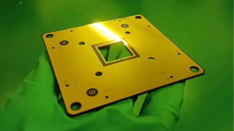
1. Patterned Inorganic Layers (Taking Through-Silicon Vias as an Example)
A photoresist pattern layer and openings are formed on a thinned wafer. The pattern is transferred to the back of the wafer using dry etching to form through-silicon vias, after which the photoresist is removed.
2. Patterned Metal Redistribution Layers
A patternless copper layer is first electroplated onto the wafer surface. A patterned photoresist layer is then formed using photolithography. The copper layer is shaped using wet etching, retaining the copper in the photoresist-covered areas and removing the copper in the opening areas. Finally, the photoresist is removed to obtain the target wiring layer.
3. Photoresist-Assisted Electroplating Process (Bump Technology)
A titanium/copper seed layer is coated onto the passivation layer surface to create a photoresist layer with openings. A wiring layer is formed on the exposed seed layer through electroplating. After electroplating, the photoresist and seed layer are removed, completing the wiring formation.
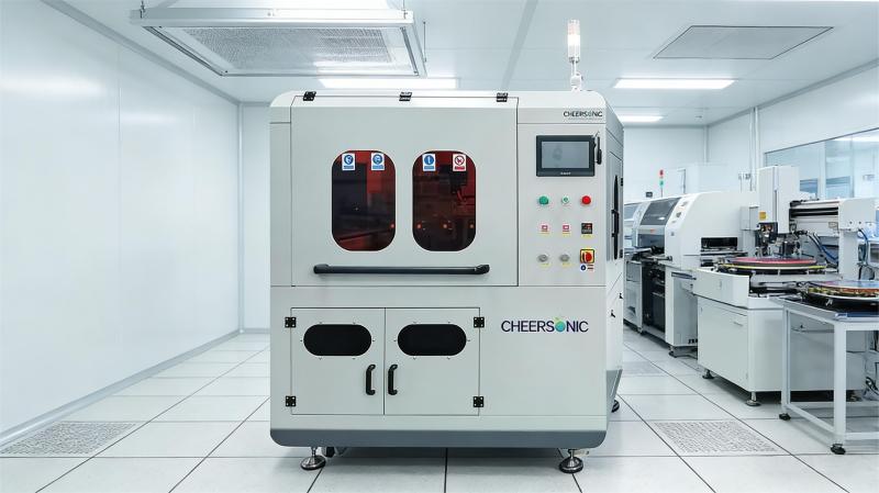
In the semiconductor chip packaging field, ultrasonic spray coating has become the mainstream precision coating process for photoresist. The equipment relies on high-frequency oscillation to atomize the photoresist into fine, uniform droplets, which are then gently deposited onto the substrate surface at low speed. This method is perfectly suited for various scenarios such as fan-out packaging, TSV through-hole packaging, and MEMS device packaging. Compared to traditional spin coating processes, this method can effectively achieve full coverage coating of high aspect ratio trenches, sidewalls, and micro-hole inner walls, resulting in a uniform coating thickness without thickness deviations or photoresist accumulation. It also significantly improves photoresist utilization, reduces material waste, precisely controls film thickness, improves the accuracy of subsequent photolithography etching, and reduces the defect rate in the packaging process. Its process stability is strong, and its adaptability is wide, meeting the needs of miniaturized, high-density advanced packaging production. It effectively simplifies the process flow and helps the semiconductor packaging industry steadily develop towards high precision, high efficiency, and low cost.
About Cheersonic
Cheersonic is the leading developer and manufacturer of ultrasonic coating systems for applying precise, thin film coatings to protect, strengthen or smooth surfaces on parts and components for the microelectronics/electronics, alternative energy, medical and industrial markets, including specialized glass applications in construction and automotive.
Our coating solutions are environmentally-friendly, efficient and highly reliable, and enable dramatic reductions in overspray, savings in raw material, water and energy usage and provide improved process repeatability, transfer efficiency, high uniformity and reduced emissions.
Chinese Website: Cheersonic Provides Professional Coating Solutions