A Critical Step in PCB Copper Fill Design
A Critical Step in PCB Copper Fill Design – Ultrasonic Soldering Lab Trials – Sonic4Lab
In PCB design, copper fill is a crucial step in covering unused areas with copper, significantly impacting circuit performance. Its core functions include reducing ground line impedance to enhance anti-interference capabilities, reducing voltage drop on power supply lines to improve efficiency, and reducing loop areas by connecting to ground lines.
Copper fill offers significant advantages. Regarding electromagnetic compatibility, large areas of copper fill for ground or power supply circuits can shield interference and enhance anti-interference capabilities. Regarding process engineering, it ensures uniform electroplating, reduces board deformation during lamination, and improves manufacturing quality. Regarding signals, it provides a return path for high-frequency digital signals, reduces DC network wiring, and enhances transmission stability. Regarding heat dissipation, proper design can improve heat dissipation and reduce device temperatures. It can also assist in the installation of specialized components, increase PCB stability, and minimize deformation. Especially for double-sided or multi-layer boards, it can help match thermal expansion coefficients and increase strength.
However, copper fill also has its drawbacks. If component pins are fully covered, copper’s high thermal conductivity can make soldering and rework difficult. This can be mitigated by using a “cross-shaped solder pad.” Copper plating around antennas can weaken signals and cause interference, and copper plating is also not recommended around amplifier circuits. Improper design can also increase processing complexity, but fortunately, existing processes are mature and the impact is minimal.
Copper plating mainly comes in two types: solid and mesh. Solid copper plating offers excellent conductivity and shielding, making it suitable for high-frequency, high-speed signals and dissipating heat well. However, it increases PCB weight and can cause warping and blistering during wave soldering, requiring slotting. Mesh copper plating offers slightly poorer shielding and heat dissipation, with weaker current flow capacity, potentially increasing high-frequency signal transmission losses. However, it reduces weight and offers greater flexibility in coping with thermal expansion and mechanical stress.
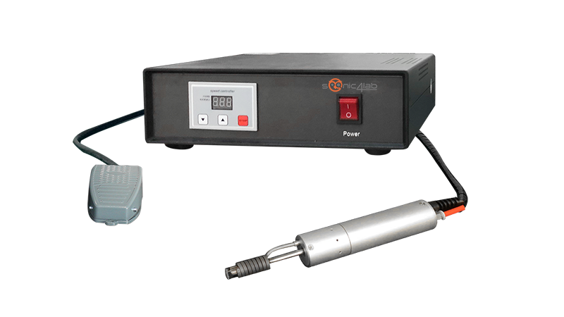
The choice of copper plating method depends on design requirements. Solid copper plating is recommended when conductivity, shielding, heat dissipation, or high-frequency, high-speed signals are important. Mesh copper plating is more suitable when weight and cost are important, or when environmental stresses are complex. Proper application of copper plating techniques can significantly improve PCB performance and reliability. Ultrasonic soldering irons, with their core advantage of flux-free soldering, demonstrate irreplaceable value in precisely connecting thin gold ribbons to gold-plated pads on PCBs. When working with thin gold ribbons as thin as 250μm and tiny gold-plated pads measuring approximately 2mm, they eliminate the need for flux to remove the oxide layer. Instead, they utilize high-frequency mechanical vibrations of 20kHz-40kHz to induce plastic deformation at the soldering interface. This, combined with localized high temperatures, breaks down and peels off the oxide layer on the metal surface, directly achieving atomic bonding between the gold ribbon and the gold-plated pad.
If you want to purchase equipment, please click here