Can Vias be Drilled Through Pads?
In PCB design, whether vias are necessary depends on the specific scenario and process.
In some cases, drilling vias through pads is necessary. For example, to improve heat dissipation for large devices like MOSFETs, vias are often drilled on the backside of the pads. In this case, the holes should be evenly spaced to ensure uniform heating. However, the biggest problem with this approach is that solder can escape through the vias, resulting in insufficient solder and poor soldering.
Drilling vias through pads is generally not recommended for components like resistors and capacitors with small packages. These components are prone to “tombstone” during reflow soldering—unbalanced surface tension on the pads at both ends can cause the component to lift and desolder. Drilling vias through pads exacerbates this tension imbalance, increasing the risk of “tombstone” and should therefore be avoided.
There are two opposing views on pad drilling. Supporters believe that in areas with limited space or complex routing, drilling vias through pads can enhance current handling and heat dissipation. Simply apply green paint to the backside of the vias to prevent solder leakage. Opponents point out that traditional processes can cause solder to flow into vias, leading to cold solder joints. While microvias and plugging can address this issue, they are costly.
Drilling vias in pads has distinct advantages and disadvantages. The advantages are that it facilitates trace routing and reduces parasitic inductance in the vias. The disadvantages are that it can easily cause cold solder joints during reflow soldering. On double-sided SMD boards, solder paste bleed-out can also cause short circuits in the pads on the reverse side.
The key to resolving soldering issues with vias in pads lies in the plugging process. Common methods include plugging vias after hot air leveling, plugging vias before hot air leveling (e.g., transferring pattern data after plugging vias in aluminum sheets, or directly silkscreening solder mask), and performing both solder mask and plugging on the board simultaneously. These processes can reduce solder paste loss and the risk of short circuits by blocking the vias, but careful control of process parameters is crucial to avoid problems such as voids, unevenness, and solder beads.
Whether or not vias can be drilled in pads is not absolute; it requires a balance between design requirements and process costs. As a last resort, appropriate plugging processes can be used, but soldering reliability must be carefully evaluated. If conditions permit, avoid drilling holes in pads and resolve routing issues through optimized layout.
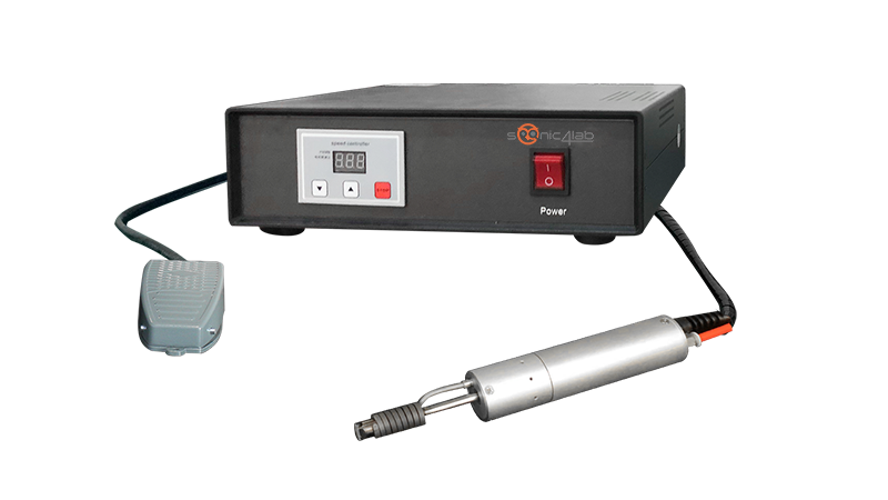
Ultrasonic soldering machines, with their core advantage of flux-free soldering, demonstrate irreplaceable value in precisely connecting thin gold ribbons to gold-plated PCB pads. When working with thin gold ribbons just 250μm wide and tiny gold-plated pads measuring approximately 2mm, they eliminate the need for flux to remove the oxide layer. Instead, they utilize high-frequency mechanical vibrations of 20kHz-40kHz to induce plastic deformation at the soldering interface under the action of energy. This simultaneously generates localized high temperatures, breaking and peeling off the oxide layer on the metal surface, and directly achieving atomic bonding between the gold ribbon and the gold-plated pad.
If you want to purchase equipment, please click here